- 您现在的位置:买卖IC网 > Sheet目录364 > SST25WF040-40-5I-QAE-T (Microchip Technology)IC FLASH SER 4MB 40MHZ SPI 8WSON
512 Kbit / 1 Mbit / 2 Mbit / 4 Mbit 1.8V SPI Serial Flash
A Microchip Technology Company
SST25WF512 / SST25WF010 / SST25WF020 / SST25WF040
Data Sheet
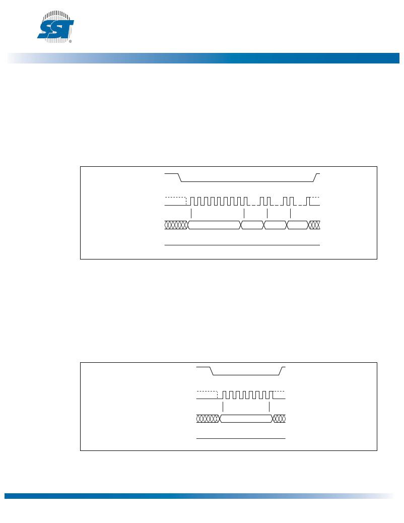
64-KByte Block-Erase for SST25WF020 and SST25WF040
The Block-Erase instruction clears all bits in the selected 64 KByte block to FFH. A Block-Erase
instruction applied to a protected memory area is ignored. Prior to any Write operation, the Write-Enable
(WREN) instruction must be executed. CE# must remain active low for the duration of any command
sequence. The Block-Erase instruction is initiated by executing an 8-bit command, D8H, followed by
address bits [A 23 -A 0 ]. Address bits [A MS -A 16 ] (A MS = Most Significant Address) are used to determine
block address (BA X ), remaining address bits can be V IL or V IH. CE# must be driven high before the instruc-
tion is executed. Poll the Busy bit in the software status register or wait T BE for the completion of the inter-
nal self-timed Block-Erase. See Figure 15 for the Block-Erase sequences.
CE#
MODE 3
0 1 2 3 4 5 6 7 8
15 16
23 24
31
SCK
MODE 0
SI
D8
ADDR
ADDR
ADDR
SO
MSB
MSB
HIGH IMPEDANCE
1328 F15.0
Figure 15: 64-KByte Block-Erase Sequence
Chip-Erase
The Chip-Erase instruction clears all bits in the device to FFH. A Chip-Erase instruction is ignored if
any of the memory area is protected. Prior to any Write operation, the Write-Enable (WREN) instruction must
be executed. CE# must remain active low for the duration of the Chip-Erase instruction sequence. The
Chip-Erase instruction is initiated by executing an 8-bit command, 60H or C7H. CE# must be driven high
before the instruction is executed. The user may poll the Busy bit in the software status register or wait T CE
for the completion of the internal self-timed Chip-Erase cycle. See Figure 16 for the Chip-Erase
sequence.
CE#
MODE 3
0 1 2 3 4 5 6 7
SCK
SI
SO
MODE 0
60 or C7
MSB
HIGH IMPEDANCE
1328 F16.0
Figure 16: Chip-Erase Sequence
?2011 Silicon Storage Technology, Inc.
19
DS25016A
06/11
发布紧急采购,3分钟左右您将得到回复。
相关PDF资料
SST25WF080-75-4I-ZAE
IC FLSH SER 8MB 75MHZ SPI 8CSP
SST26VF032A-80-5I-S2AE
IC FLASH 32MBIT 8SOIC
SST38VF6402-90-5I-B3KE-T
IC FLASH MPF 64MBIT 90NS 48TFBGA
SST39LF802C-55-4C-MAQE-T
IC FLASH MPF 8MBIT 48-WFBGA
SST39SF040-70-4C-WHE
IC FLASH MPF 4MBIT 70NS 32TSOP
SST39VF1602C-70-4I-B3KE
IC FLASH MPF 16MBIT 70NS 48TFBGA
SST39VF200A-70-4I-MAQE
IC FLASH MPF 2MBIT 70NS 48-WFBGA
SST39VF3201-70-4I-B3KE-T
IC FLASH MPF 32MBIT 70NS 48TFBGA
相关代理商/技术参数
SST25WF040-40-5I-QAF
制造商:SST 制造商全称:Silicon Storage Technology, Inc 功能描述:512 Kbit / 1 Mbit / 2 Mbit / 4Mbit 1.8V SPI Serial Flash
SST25WF040-40-5I-SAE
制造商:SST 制造商全称:Silicon Storage Technology, Inc 功能描述:512 Kbit / 1 Mbit / 2 Mbit / 4Mbit 1.8V SPI Serial Flash
SST25WF040-40-5I-SAF
功能描述:闪存 4M (512Kx8) 40MHz Industrial Temp RoHS:否 制造商:ON Semiconductor 数据总线宽度:1 bit 存储类型:Flash 存储容量:2 MB 结构:256 K x 8 定时类型: 接口类型:SPI 访问时间: 电源电压-最大:3.6 V 电源电压-最小:2.3 V 最大工作电流:15 mA 工作温度:- 40 C to + 85 C 安装风格:SMD/SMT 封装 / 箱体: 封装:Reel
SST25WF040-40-5I-SAF-T
功能描述:闪存 1.65 to 1.95V 4Mbit SPI Serial 闪存 RoHS:否 制造商:ON Semiconductor 数据总线宽度:1 bit 存储类型:Flash 存储容量:2 MB 结构:256 K x 8 定时类型: 接口类型:SPI 访问时间: 电源电压-最大:3.6 V 电源电压-最小:2.3 V 最大工作电流:15 mA 工作温度:- 40 C to + 85 C 安装风格:SMD/SMT 封装 / 箱体: 封装:Reel
SST25WF080
制造商:SST 制造商全称:Silicon Storage Technology, Inc 功能描述:8Mbit 1.8V SPI Serial Flash
SST25WF080_12
制造商:MICROCHIP 制造商全称:Microchip Technology 功能描述:8 Mbit 1.8V SPI Serial Flash
SST25WF080-75-4I-SAE
制造商:SST 制造商全称:Silicon Storage Technology, Inc 功能描述:8Mbit 1.8V SPI Serial Flash
SST25WF080-75-4I-SAF
功能描述:闪存 8M (1Mx8) 75MHz Industrial Temp RoHS:否 制造商:ON Semiconductor 数据总线宽度:1 bit 存储类型:Flash 存储容量:2 MB 结构:256 K x 8 定时类型: 接口类型:SPI 访问时间: 电源电压-最大:3.6 V 电源电压-最小:2.3 V 最大工作电流:15 mA 工作温度:- 40 C to + 85 C 安装风格:SMD/SMT 封装 / 箱体: 封装:Reel
